
793353
Tungsten oxide (WO3-x) nanoparticle ink
Synonym(s):
Tungsten oxide nanoparticle dispersion, Tungsten oxide suspension, WO3 dispersion, WO3 ink, Tungsten oxide, Tungsten oxide nanoparticle
Select a Size
About This Item
form
dispersion
Quality Level
concentration
2.5 wt. % in 2-propanol
particle size
<50 nm (BET)
density
0.7992 g/mL at 25 °C
General description
Annealing temperature <100°C.
Application
Other Notes
Working conditions: Application and film drying under nitrogen (or low humidity)
Post-treatment: Annealing of deposited WO3-x films at 80°C - 120°C
Legal Information
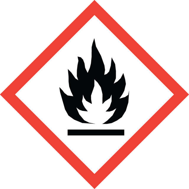

signalword
Danger
hcodes
Hazard Classifications
Eye Irrit. 2 - Flam. Liq. 2 - STOT SE 3
target_organs
Central nervous system
Storage Class
3 - Flammable liquids
wgk
WGK 1
flash_point_f
53.6 °F - closed cup
flash_point_c
12 °C - closed cup
Regulatory Information
This item has
Choose from one of the most recent versions:
Already Own This Product?
Find documentation for the products that you have recently purchased in the Document Library.
Articles
Progress in solution-processed functional materials leads to thin-film optoelectronic devices for industrial and consumer electronics.
Professors Tokito and Takeda share design principles and optimization protocols for organic electronic devices, focusing on flexibility and low cost.
Find advantages of inorganic interface layer inks for organic electronic & other applications.
Global Trade Item Number
| SKU | GTIN |
|---|---|
| 793353-5ML | 04061838085528 |
| 793353-25ML | 04061838103239 |
| 793353-50ML | 04061835435654 |